We introduced
the use of functionalized SWNTs, lying-down on metal surfaces, as efficient linking
spacers between redox proteins and metal surfaces,
for biodevice application, for two main reasons:
- a
direct metal-protein interaction could induce the protein denaturation
[1], and this can be overcome by introducing organic molecules as linking
spacers [2,3];
- the conduction perpendicular to the main nanotube axis (transverse conduction) should occur over a
carrier path shorter than the phonon scattering mean free path (the diameters
ranging between 0.5 and 5 nm), and then, an efficient electrical conjugation is
expected between proteins and metal surfaces when connected by a lying-down
SWNT.
Molecular Topographic Properties
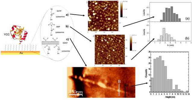
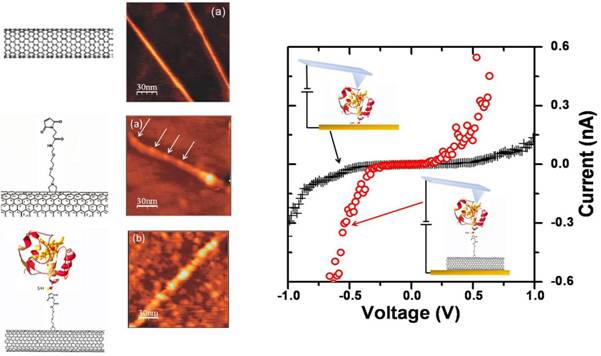
Yeast Cytochrome c (YCC) molecules directly adsorbed on a gold
surface, images in TM-AFM in fluid, show a mean height of 2.6 nm, with respect
to a crystallographic size of 3.4 nm [4]. We verified that the introduction of
an organic linker spacer allows YCC proteins to recover their original size, in
three different cases: by using organic chains, such as SATP or SMP, or oxidized
SWNTs [2].
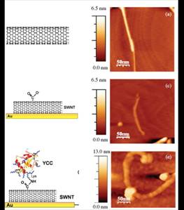
To achieve protein electrostatical
adsorbtion of SWNT sidewalls, these latter have to be
treated with acid solution, in order to create carboxylic groups on their
sidewalls, which electrostatically bound the lysine
residues of proteins. Such a bond can also become covalent, if properly
activated [5], without changing the protein topography.
SWNT Transverse Conduction Properties
A new metode
based on Current Sensing AFM (CS-AFM) has been introduced to discriminate metallic from semiconducting SWNTs
(when lying on a conductive substrate) [6]. This method is mainly based
on the concept of transverse current, i.e. the current across the SWNT as
measured in the direction perpendicular to the main nanotube axis.
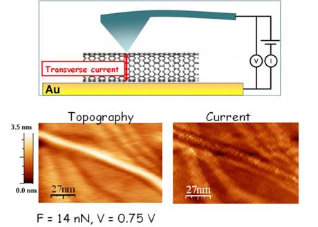
Indeed, both the contrast in current imaging and the trend of the
current response as a function of the applied force depend on the electronic
character of the SWNT analyzed.
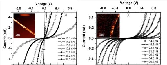
Within the framework of a tunneling transport model, the
data have shown that, at applied bias in the ±1 V range, for semiconductor
SWNTs the transport is always tunneling-like, while for the metallic ones, it
switches from tunneling to band-like, to tunneling again, with increasing the
applied force load, being the second switching probably due to the nanotube deformation induced by the mechanical stress [6].
SWNTs as electrically efficient linkers
Their capability of
preserve the original protein crystallographic size and their peculiar
transverse conduction properties, allow metallic SWNTs to play a predominant
role in increasing the electronic coupling between proteins adsorbed on their
sidewalls and the underlying metal electrode. By means of CS-AFM, we measured
also the conduction across metallic SWNTs covalently coated with YCC molecules and
we compared it with that across single YCC molecules directly chemisorbed on a
gold surface. We obtained that the electrical coupling between the redox protein and the metal surface is enhanced when a
metallic SWNTs is used as covalent linking spacer, due to the participation of
their electronic band to the transverse transport across the hybrid system [5,7].
Such an effect has been
observed twice, for two different covalent immobilizations of the YCC proteins
on the metallic SWNT sidewalls: (1) oxidation of the nanotubes
and subsequent activation of the amide bond formation among the carboxylic
groups on the nanotube sidewalls and the Lysine
residues of the protein surface [5]; (2) functionalization
of the SWNTs with organic chains maleimide-terminated,
in order to control the protein-to-nanotube (i.e. the
protein-to-surface) orientation by targeting the thiol
groups, which are scarcely present on the protein surfaces [7].
[1] D. L. Johnson,
C. J. Maxwell, D. Losic, J. G. Shapter,
and L. L. Martin, Bioelectrochem. 58, (202) 137. [2] I. Delfino, B. Bonanni, L. Andolfi, C. Baldacchini, A. R. Bizzarri, and S. Cannistraro, J. Phys.: Condens. Matter 19, (2007) 225009.
[3] B. Bonanni, A.
R. Bizzarri, and S. Cannistraro, J. Phys. Chem. B 110, (2006) 14574.
[4] Bonanni et al.,
CHEMPHYSCHEM 4, (2003) 1183.
[5] C.
Baldacchini, and S. Cannistraro, J. Nanosci. Nanotech.
10 (2010) 2753.
[6] C.
Baldacchini, and S. Cannistraro, Appl.
Phys. Lett. 91, (2007) 122103.
[7]
C. Baldacchini, M. A. Herrero Chamorro,
M. Prato, and S. Cannistraro, Adv.
Funct. Mat. 21 (2011) 153.